The preparation process for silicon carbide (SiC) substrates is complex and technically challenging, involving specific critical steps such as raw material synthesis, crystal growth, ingot processing, crystal cutting, wafer grinding, wafer polishing, wafer inspection, and final wafer cleaning. Leading SiC wafer suppliers master this intricate production chain to deliver high-quality substrates. HMT typically supply 4 inch to 8 inch SiC wafer products in both conductive type and semi-insulating type to meet diverse application needs in power electronics and RF devices. The market offers these wafers with competitive pricing, influenced by factors like crystal quality, defect density, and polishing level. For procurement, it's essential to consult reliable SiC wafer suppliers who provide full specification sheets, including detailed parameters for bow, warp, TTV, and surface roughness, ensuring the wafers meet specific technical requirements.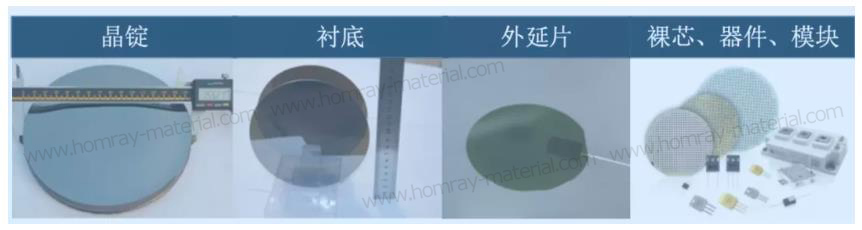
Raw Material Synthesis
High-purity silicon powder and high-purity carbon powder are uniformly mixed in a specific ratio. The mixture is then processed in a high-temperature reaction chamber exceeding 2000°C to synthesize silicon carbide particles with a specific crystal structure and particle size. The resulting material undergoes crushing, sieving, cleaning, and other steps to produce high-purity silicon carbide powder that meets the requirements for crystal growth.
Crystal Growth
Crystal growth is the most technically challenging step in the manufacturing of silicon carbide substrates, directly determining the electrical properties of the substrate. Mainstream crystal growth methods currently include the Physical Vapor Transport (PVT) method, High-Temperature Chemical Vapor Deposition (HTCVD) method, and Liquid-Phase Epitaxy (LPE) method.
Among these, the PVT method is the mainstream commercial process for producing SiC substrates, known for its technological maturity and widespread engineering applications. The LPE method is considered a potential future direction. In the PVT method, high-purity silicon carbide micropowder and a seed crystal are placed in the lower and upper parts of a graphite crucible within a single-crystal growth furnace, creating an axial temperature gradient. The silicon carbide micropowder sublimates at high temperatures into gas-phase components such as Si₂C, SiC₂, and Si, which are transported to the seed crystal under the temperature gradient to nucleate and crystallize, ultimately forming a silicon carbide ingot.
Although the PVT method offers relatively low growth costs, its primary challenge lies in obtaining high-purity SiC raw materials, as trace impurities can significantly affect crystal purity.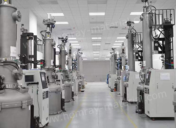

SiC Ingot Processing
An X-ray single-crystal orientation system is used to orient the silicon carbide ingot. The ingot is then subjected to precision machining to flatten and round it into a standard-diameter silicon carbide crystal rod with specific angles. All rods undergo dimensional and angular inspections.
SiC Ingot Cutting
With allowances made for subsequent processing, the crystal rod is sliced into wafers of varying thicknesses using diamond wire cutting. Fully automated testing equipment is employed to inspect surface parameters such as warp, bow, and total thickness variation (TTV).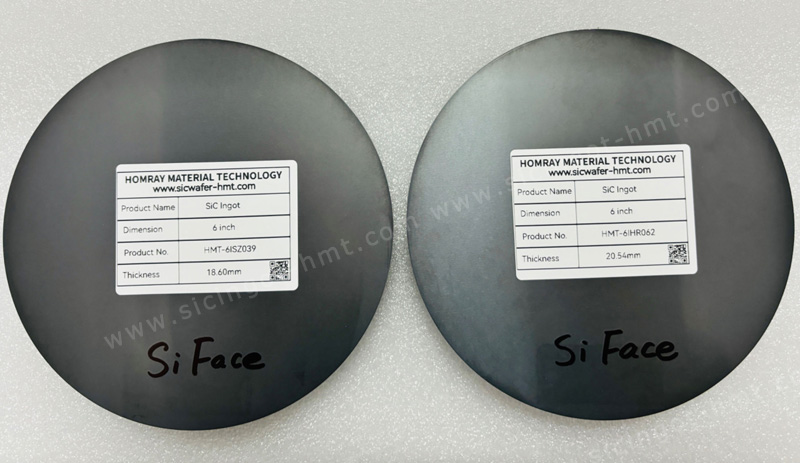
Grinding of Sliced Wafers
The sliced wafers are thinned to a specified thickness using specialized grinding slurry, removing surface wire marks and damage. All sliced wafers are inspected for surface morphology and electrical properties using fully automated testing equipment and non-contact resistivity testers.
Polishing of SiC Wafers
Specific polishing slurries are used for mechanical and chemical polishing of the ground wafers to eliminate surface scratches, reduce roughness, and remove processing stress, achieving nanometer-level surface flatness.Parameters are inspected using equipment such as X-ray diffractometers, atomic force microscopes, surface flatness testers, and surface defect integrated testers to determine the quality grade of the polished wafers.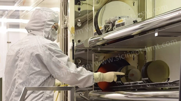
Cleaning of Polished Wafers
In a Class 100 cleanroom, the polished wafers are cleaned using specific chemical reagents and deionized water to remove surface particles, metal ions, and organic contaminants. After spin-drying, they are packaged in clean wafer cassettes, resulting in the final silicon carbide substrates.
CATEGORIES
LATEST NEWS
- Introduction to the main functions of PbootCMS
Further Application of SiC Power Devices In New Energy Vehicles
- Introduction to the main functions of PbootCMS
SiC Wafer Manufacturer Production Analysis
- Introduction to the main functions of PbootCMS
Silicon Carbide SiC Wafer Polishing New Direction
- Introduction to the main functions of PbootCMS
SiC Boules and SiC Substrates industry chain
CONTACT US
Contact: Mr.Kimrui
Phone: 15366208370
Tel: 15366208370
Email: kim@homray-material.com
Add: LiSheng Industrial Building, 60SuLi Road, WuZhong District, JiangSu Province, P.R.China.