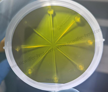
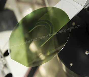
2 inch SiC Substrate Wafer Manufacturer
Althrough 2 inch SiC Wafer almost stop production for SiC Wafer Manufacturer, but HMT company still can provide 50.8mm 2 inch SiC Substrate wafer for ...
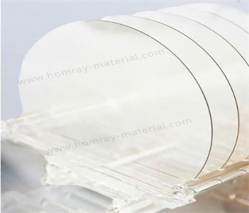
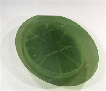
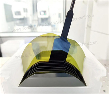
Although most of SiC Wafer Manufacturers has stopped 2 inch SiC Substrate Wafer production, but HMT company still can provide 50.8mm 2 inch SiC Substrate wafer for worldwide customers. We keep few capacity allocation for 2 inch SiC wafer , 2 inch As cut SiC wafer and 2 inch SiC Boules. We only have Conductive N type for all 2 inch SiC products now but we support customization. For example, if you need 2 inch Raw cut SiC wafer thickness>1000um you can contact HMT. If you need 2 inch SiC Substrate thickness 350um TTV < 10um you can contact HMT etc.
2 inch SiC Polished Wafer 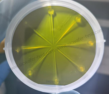
From the perspective of electrochemical property differences, SiC substrate materials can be divided into conductive substrates (resistivity range 15~30mΩ·cm) and semi-insulated substrates (resistivity higher than 105Ω·cm).
Semi-insulated SiC substrate is mainly used in the manufacture of radio frequency devices, photoelectric devices, etc.
Conductive SiC substrate is mainly used in the manufacture of Schottky diodes, MOSFETs, IGBTs and other power devices.

CATEGORIES
LATEST NEWS
- Introduction to the main functions of PbootCMS
Further Application of SiC Power Devices In New Energy Vehicles
- Introduction to the main functions of PbootCMS
SiC Wafer Manufacturer Production Analysis
- Introduction to the main functions of PbootCMS
Silicon Carbide SiC Wafer Polishing New Direction
- Introduction to the main functions of PbootCMS
SiC Boules and SiC Substrates industry chain
CONTACT US
Contact: Mr.Kimrui
Phone:
Tel: Please send your detailed inquiry or requirements via email below.
Email: kim@homray-material.com
Add: Please send your detailed inquiry or requirements via email below.