
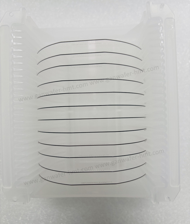
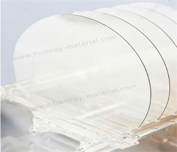
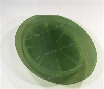
Semi-insulating SiC Wafer For GaN-ON-SiC Epi Wafer
Achieve high-quality GaN epitaxy on SiC with HMT's high-purity 4H-SiC wafers (4" to 8"). Minimize defects, step bunching, and anisotropy using optimiz...
To obtain high-quality SiC-based GaN epitaxy wafer and devices, a 4° off-axis SiC Substrate can lead to step bunching, surface roughness, reduced crystal quality, and anisotropic electrical performance in GaN epitaxial layers. For such applications, HMT can supply high purity 4H-SiC wafers from 4 inch to 8 inch for growing high-quality GaN epi layers. Furthermore, prior to growing the AlN layer, high-temperature gas treatment of the SiC substrate is necessary.
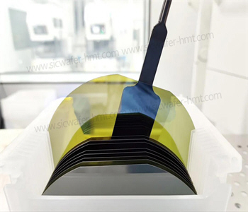
Semi-insulating SiC Wafer GaN on SiC Epi Wafer Pictures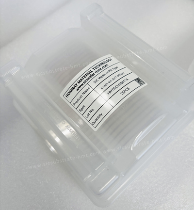
Common solutions include:
Introducing an AlN buffer layer to improve the wetting layer on the SiC surface, regulate stress, and block the propagation of substrate defects into the GaN epitaxial layer, thereby enhancing the quality of the GaN epitaxial layer.
Prior to growing the AlN layer, high-temperature gas treatment of the SiC substrate is necessary. Surface treatment of the SiC substrate is one of the critical challenges in GaN epitaxy on SiC substrates. In the early stages, issues such as scratches, sub-surface damage layers, and residual contaminants from the SiC substrate cutting, grinding, and polishing processes, along with surface oxide layers, sub-surface damage layers, and defects, adversely affected the quality of GaN epitaxial layers. Due to the poor wetting behavior of Ga atoms on the SiC substrate surface, direct growth of GaN on SiC results in slow growth rates and poor material quality. Additionally, the mismatch in lattice constants and thermal expansion coefficients between SiC and GaN subjects the GaN layer to compressive stress during growth. The difference in thermal expansion coefficients further induces tensile stress in the GaN film during post-growth cooling. These stresses lead to high-density defects in the GaN epitaxial layer.
To address issues such as stacking fault (SF) defects, poor Ga atom wettability, lattice mismatch, and thermal mismatch in GaN epitaxy on SiC substrates, strategies including the introduction of buffer layers (such as AlN, AlGaN, AlN/GaN, SiNx) and patterned substrates have been employed to improve GaN film quality.
In recent years, GaN/SiC hybrid transistors have become a research hotspot. They combine the high mobility and switching speed of GaN with the high thermal conductivity and avalanche resistance of SiC, while achieving no dynamic on-resistance degradation and excellent thermal stability.

CATEGORIES
LATEST NEWS
- Introduction to the main functions of PbootCMS
Further Application of SiC Power Devices In New Energy Vehicles
- Introduction to the main functions of PbootCMS
SiC Wafer Manufacturer Production Analysis
- Introduction to the main functions of PbootCMS
Silicon Carbide SiC Wafer Polishing New Direction
- Introduction to the main functions of PbootCMS
SiC Boules and SiC Substrates industry chain
CONTACT US
Contact: Mr.Kimrui
Phone:
Tel: Please send your detailed inquiry or requirements via email below.
Email: kim@homray-material.com
Add: Please send your detailed inquiry or requirements via email below.